
Fujifilm already let us know that there would be a new stacked sensor coming for the Fujifilm X-H2 during the X-Summit and to expect it at the next X-Summit which will be occurring in May. Now a patent has surfaced explaining what we can expect from this new stacked X-Trans CMOS.
The patent seems to indicate we may finally be getting smooth blackout-free or blackout-reduced live view while shooting continuously thanks to the camera’s ability to output image files and run live view in parallel with the new processor/stacked CMOS combo.
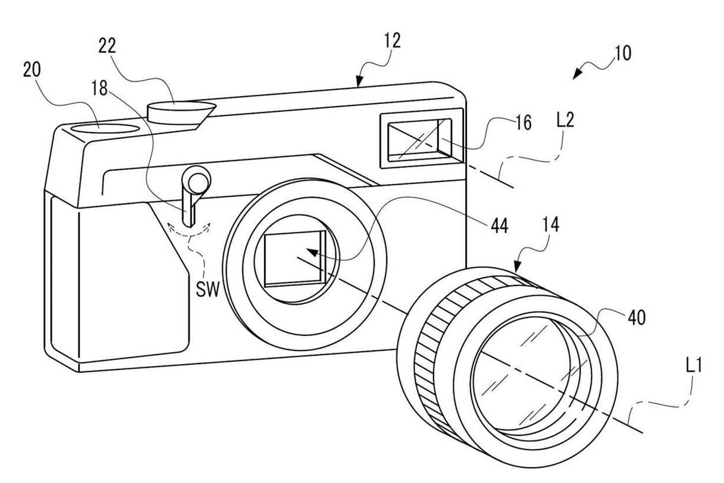
Below you can find some of the translated patent in addition to translated patent images:
[Patent Claims]
[Claim 1]
Processor,
An imaging device includes a memory built in or connected to the processor, and a memory.
The processor and the memory are incorporated in the imaging element.
The processor has a 1 communication interface and a 2 communication interface.
The 1 communication interface outputs image data obtained by capturing an image of an object to a 1 external processor disposed outside the imaging element as the 1 image data.
The memory stores the image data.
The 2 communication interface outputs the image data stored in the memory as 2 image data to a 2 external processor.
The output system of the 1 communication interface is different from the output system of the 2 communication interface.
The 1 communication interface outputs the image data transferred without passing through the memory as the 1 image data.
An image pickup device.
[Claim 2]
The imaging device according to claim 1, wherein output of the 1 image data by the 1 communication interface and output of the 2 image data by the 2 communication interface are performed independently of each other.
[Claim 3]
The imaging device according to claim 1, wherein the 1 communication interface outputs the 2 image data in a period different from an output period of the 2 image data by the 1 communication interface.
[Claim 4]
The imaging device according to claim 3, wherein the 2 communication interface outputs the 2 image data in response to a request from the external processing unit.
[Claim 5]
The imaging device according to claim 3 or 4, wherein the output period is a vertical blanking period after the 1 image data for 1 frames is output from the 1 communication interface.
[Claim 6]
The imaging device according to claim 3 or 4, wherein the output period is a vertical blanking period before the 1 image data for 1 frames is output from the 1 communication interface.
[Claim 7]
The imaging device according to claim 3 or 4, wherein the output period is a horizontal blanking period after the 1 image data for 1 lines is output from the 1 communication interface.
[Claim 8]
The imaging device according to claim 3 or 4, wherein the output period is a horizontal blanking period before the 1 image data for 1 lines is output from the 1 communication interface.
[Claim 9]
The device includes a 1 A / D converter for performing A / D conversion of analog image data.
The imaging device according to claim 3 or 4, wherein the output period is an A / D conversion period by the 1 A / D converter before the 1 image data for 1 lines is output from the 1 communication interface.
[Claim 10]
The device includes a 2 A / D converter for performing A / D conversion of analog image data.
The processor includes a memory controller which causes the memory to store digital image data obtained by digitizing the analog image data by the 2 A / D converter.
The output of the 1 communication interface is obtained from the 2 A / D converter.The output system outputs the digital image data as the 1 image data without storing the digital image data in the memory.
An imaging device according to any one of claims 1 to 9, wherein an output method of the 2 communication interface is an output method of outputting the digital image data read from the memory by the memory controller as the 2 image data.
[Claim 11]
An imaging device according to any one of claims 1 to 10, wherein the memory is a memory having a different write timing and a different read timing.
[Claim 12]
The imaging device of claim 11, wherein the memory is a DRAM.
[Claim 13]
An imaging device according to any one of claims 1 to 12, wherein at least the photoelectric conversion element and the memory are formed into 1 chips.
[Claim 14]
The imaging device according to claim 13, wherein the imaging element is a stacked imaging element in which the memory is stacked on the photoelectric conversion element.
[Claim 15]
An imaging device according to any one of claims 1 to 14.
A display processor for controlling the display of at least one of a 1 image based on the 1 image data output by the 1 communication interface and a 2 image based on the 2 image data output by the 2 communication interface ;
An imaging apparatus comprising :.
[Claim 16]
An imaging device according to any one of claims 1 to 14.
A storage processor for controlling a storage device to store at least one of the 1 image data output from the 1 communication interface and the 2 image data output from the 2 communication interface ;
An imaging apparatus comprising :.
[Claim 17]
A method of operating an imaging device, comprising : a processor ; a memory built into or connected to said processor ; and a 1 communication interface and a 2 communication interface.
The 1 communication interface outputs, as 1 image data, image data obtained by imaging an object to a 1 external processor disposed outside the imaging element.
The memory stores the image data.
The 2 communication interface outputs the image data stored in the memory as 2 image data to a 2 external processor.
The output system of the 1 communication interface is different from the output system of the 2 communication interface.
The 1 communication interface outputs the image data transferred without passing through the memory as the 1 image data.
An operating method of an image sensor.
[Claim 18]
A program for causing a computer to function as the 1 communication interface and the 2 communication interface, wherein a processor and a memory built in or connected to the processor are incorporated, and the processor is included in an imaging element having a 1 communication interface and a 2 communication interface, is provided.
The 1 communication interface outputs, as 1 image data, image data obtained by imaging an object to a 1 external processor disposed outside the imaging element.
The memory stores the image data.The 2 communication interface outputs the image data stored in the memory as 2 image data to a 2 external processor.
The output system of the 1 communication interface is different from the output system of the 2 communication interface.
The 1 communication interface outputs the image data transferred without passing through the memory as the 1 image data.
Program.
via J-Pat
